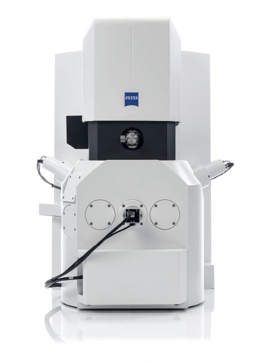
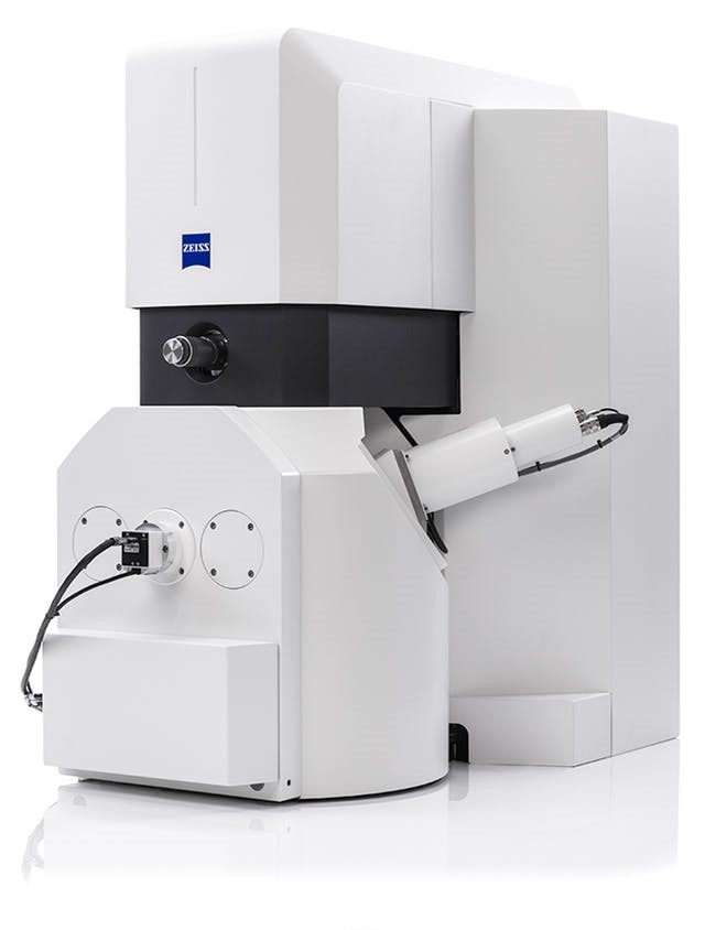
🔸 Product Overview
The ZEISS SEM EVO10 is a modern scanning electron microscope line from the Carl Zeiss brand, designed to meet the needs of analyzing material morphology and surface structure at micro and nano levels. The device stands out with its user-friendly features, flexible configuration, and superior imaging technology, making it the optimal choice for research labs, scientific institutes, and high-quality manufacturing plants. Whether you’re a materials analysis engineer, biological scientist, or industrial inspection specialist, the EVO10 can support more detailed and efficient sample observation than ever before.
🔸 Key Features
✅ Intuitive SmartSEM control interface, easy to use, allowing beginners to operate effortlessly.
✅ Integrated flexible wide vacuum chamber system, suitable for various sample sizes.
✅ Magnification range from 10x to 1,000,000x, enabling analysis from macro to nano levels.
✅ Multiple detector options: SE, BSE, EDS, supporting structural and elemental composition analysis.
✅ Auto-focus adjustment, noise compensation, and contrast optimization for enhanced image quality.
✅ Easy upgradeability with optional EDS, WDS, and EBSD modules.
🔸 Technical Specifications
| Parameter | Details |
|———–|———|
| Maximum Resolution | 3.0 nm @ 20 kV |
| Magnification Range | 10× – 1,000,000× |
| Electron Source | Tungsten or LaB6 electron gun |
| Detectors | SE (secondary electron), BSE (backscattered electron) |
| Sample Chamber Size | Up to 200 mm round or custom large samples |
| Vacuum System | Mechanical pump + molecular pump, 2 pressure modes |
| Software Interface | SmartSEM or EasySEM |
| Elemental Analysis Support | Optional EDS (Energy Dispersive X-ray) module |
| Camera/Scan System | High-resolution CCD (optional) |
🔸 Key Applications
🧪 Surface analysis in manufacturing, electronics, and nanomaterials
🧫 Biological sample observation: cells, tissues, bacteria with high detail
⚙️ Component defect inspection, material fracture analysis, coating structure evaluation
🧬 Scientific research: physics, chemistry, biology, advanced materials
🔧 Applications in metallurgy, technical ceramics, and specialty alloys
🔸 Outstanding Advantages
🌟 Superior image quality from ZEISS’s proprietary electro-optical technology.
🔧 Simple maintenance, stable operation, no complex technical requirements.
🎯 Suitable for both academic research and industrial quality control.
🧠 High automation saves time and labor.
📊 Flexible data storage and sharing via LAN or USB.
🔸 Why Choose ZEISS SEM EVO10?
✅ ZEISS brand – German excellence, trusted for over 175 years.
✅ Compact, user-friendly design supporting diverse analytical needs.
✅ EDS integration for qualitative and semi-quantitative elemental analysis.
✅ Cost-efficient operation – energy-saving and long-lasting durability.
✅ On-site training, installation, and official warranty support.
🔸 Support & Advanced Options
📦 Optional EDS module for elemental composition analysis.
🖥️ Integrated touch control display and advanced imaging software.
📁 Data recording and management for R&D organizations.
🛠️ Scheduled maintenance, spare parts supply, and on-site technical services.